CPO Is Ready for AI Data Centers. Is Testing Ready for CPO?
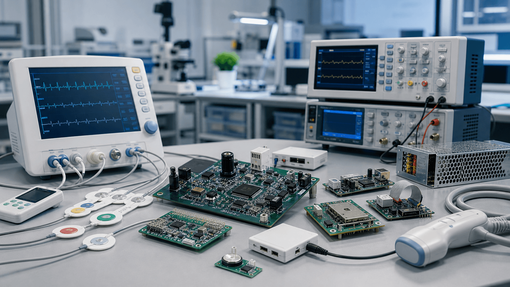
As AI data centers continue to grow, the demand for faster and more energy-efficient data transmission is increasing rapidly. Traditional electrical interconnects are facing growing limitations in bandwidth, power consumption, and latency. This is one reason why Co-Packaged Optics (CPO) and silicon photonics are attracting increasing attention as next-generation interconnect technologies. But there is a challenge that is often overlooked: CPO may be ready for commercialization, but is CPO testing ready for mass production? According to TrendForce, testing remains one of the key bottlenecks as CPO moves from the laboratory toward volume production. TSMC’s COUPE platform is also targeting volume production in 2026, further accelerating the development of the CPO ecosystem. What Makes CPO Testing So Difficult? Unlike traditional electronic IC testing, CPO combines electrical and optical technologies in the same package. A typical CPO architecture integrates a Photonic Integrated Circuit (PIC) with an Electrical Integrated Circuit (EIC). The combined component is often referred to as an Optical Engine (OE). The PIC may include: Optical couplersModulatorsPhotodetectorsOptical filtersOptical waveguides This means testing is no longer just about electrical performance. Engineers also need to measure optical parameters such as: Insertion Loss (IL)Polarization-Dependent Loss (PDL)ResponsivityWaveguide propagation lossOptical crosstalk The combination of electrical, optical, and optoelectronic testing makes CPO testing significantly more complicated than conventional IC testing. The Alignment Problem One of the biggest challenges is optical alignment. Light needs to travel from an external optical fiber into an extremely small optical waveguide. The difference in physical size is enormous. According to TrendForce, the cross-sectional area of a single-mode fiber core is approximately 78.5 µm², while the optical waveguide can be around 0.099 µm². That means the fiber core can be hundreds of times larger than the waveguide. Even a small positioning error can result in significant coupling loss. This is why CPO testing requires extremely precise alignment, together with advanced optical probes, machine vision, and automated positioning systems. Today, some of these processes still involve significant manual operations. TrendForce estimates that 100% inspection of a single PIC can take more than 100 seconds, creating a major challenge for high-volume manufacturing. Four Key Stages of
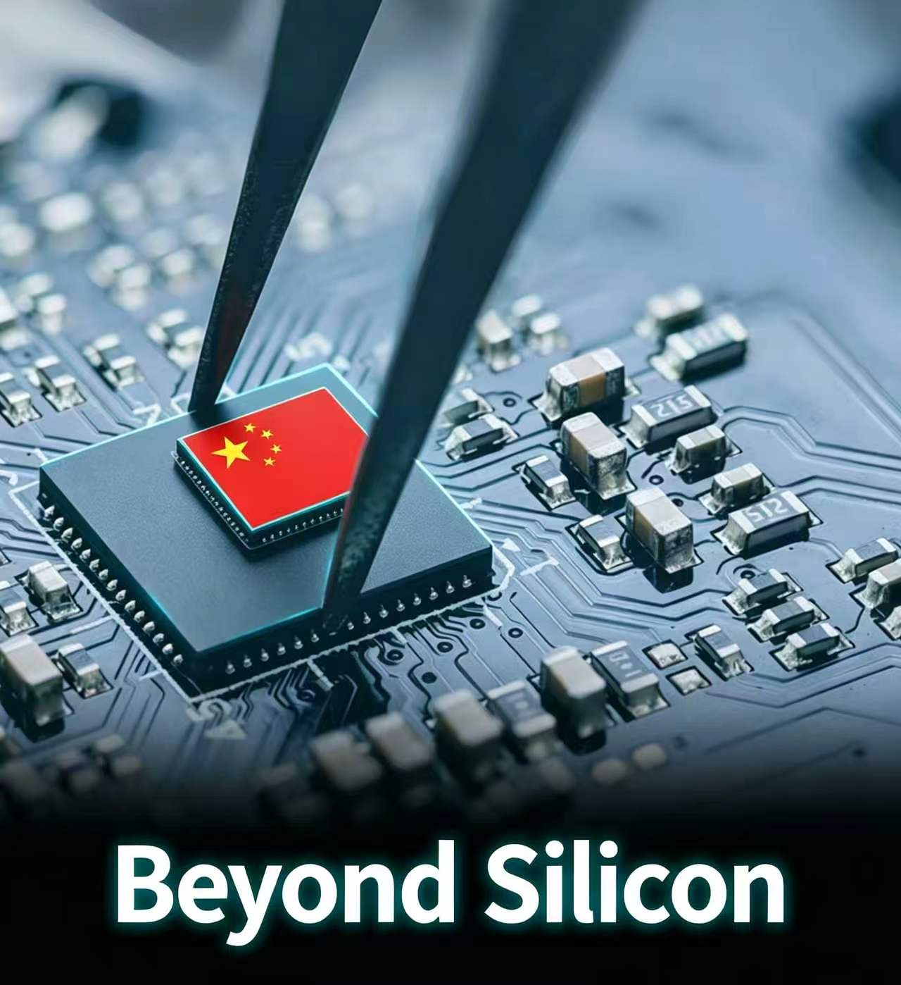
Is China Building a Future Beyond Silicon?
What if the next big breakthrough in semiconductors isn’t about making silicon smaller — but about using completely new materials? Researchers at Peking University have developed a 2D transistor based on bismuth oxyselenide using a gate-all-around (GAA) architecture. According to the reported results, it could deliver: ⚡ Up to 40% faster performance🔋 Around 10% lower energy consumption🧩 A potential alternative to traditional silicon-based transistor technology Why is this interesting? As silicon scaling becomes more challenging, researchers are looking at 2D materials as a possible new path for improving transistor performance and energy efficiency. But the real challenge is not just performance in the lab. 👉 Can 2D materials be manufactured at scale?👉 Can they be integrated into existing semiconductor processes?👉 And most importantly, can they eventually become commercial products? If these challenges can be solved, the impact could reach areas like AI chips, data centers, and next-generation electronics. The future of semiconductors may not only be about making silicon smaller. It may also be about finding what comes after silicon. 💬 What do you think?Could 2D materials become one of the next major directions in semiconductor technology?
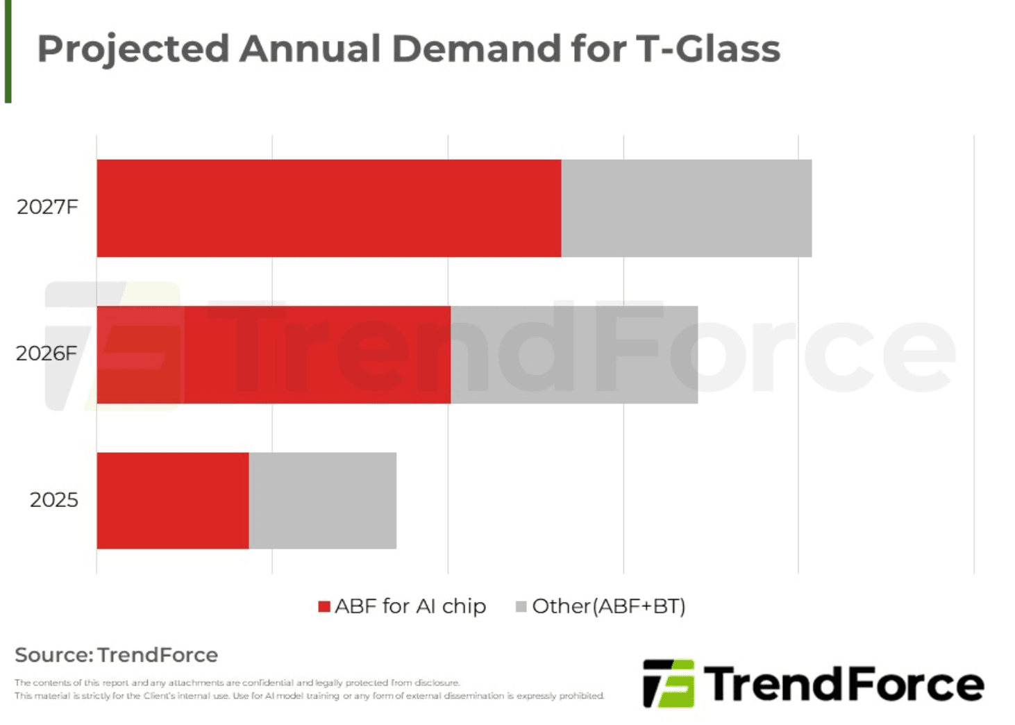
The next bottleneck in AI servers may not be the chips. It could be the materials behind them.
As AI chips and high-speed servers become more powerful, PCBs are moving toward larger sizes, more layers, and higher performance. That means higher demand for specialty fiberglass fabric. But supply is not catching up easily. 🔹 High-end weaving equipment is limited🔹 Manufacturing processes are complex🔹 New capacity takes time to come online🔹 Yield challenges reduce actual output Even with ongoing capacity expansion, high-end fiberglass fabric may remain in short supply in the near term. Quartz fiberglass fabric could offer even better signal transmission performance in the future, but its high cost and processing challenges make widespread adoption difficult for now. AI infrastructure is not just a chip story. It is also a materials, equipment, and manufacturing story. Which part of the AI supply chain do you think will face the next major bottleneck?
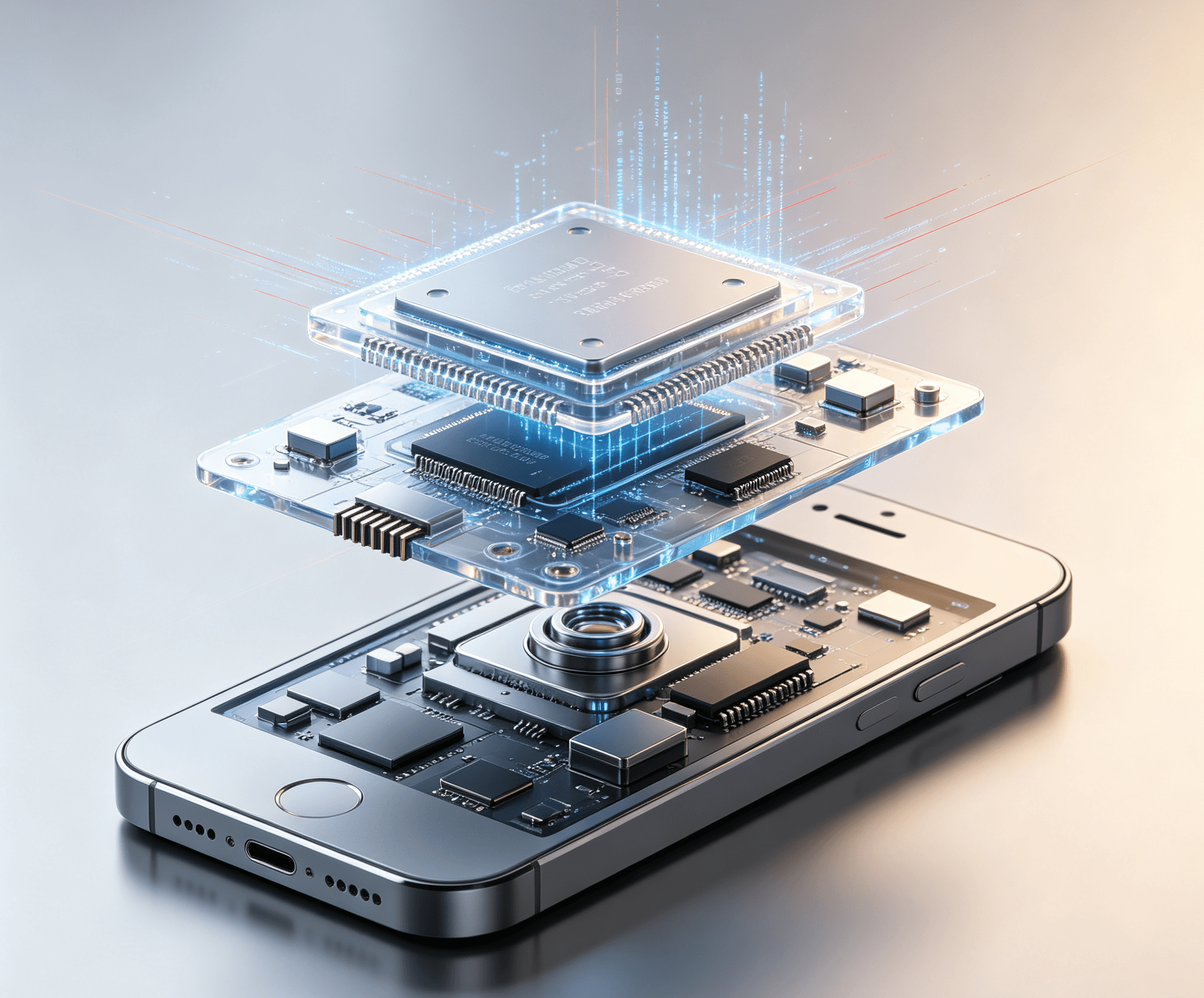
iPhone 18: Less Hardware, More AI & Pricing
The iPhone 18 is not expected to bring major hardware upgrades. The focus seems to be shifting to AI performance, pricing, and the user experience. At the same time, rising memory costs are putting more pressure on Apple’s BOM and profit margins. It will be interesting to see how Apple balances hardware costs, pricing, and AI to drive sales.

Humanoid Robots Are Entering a New Stage
The humanoid robot industry is moving fast. In 2026, the focus is shifting from technology validation to early commercialization. China, North America, and Asia’s supply chain are all pushing the industry forward. The competition is no longer just about the robot itself. It’s about AI models, key components, computing power, and the supply chain behind them. Humanoid robots are becoming one of the key applications of Physical AI. It will be interesting to see how this industry develops from here.

Is This the Next DeepSeek Moment?
China’s open-source AI race is moving fast. On July 27, Moonshot AI officially open-sourced the weights of its flagship model, Kimi K3. With 2.8 trillion total parameters, it is now one of the largest open-source AI models in the world. And the momentum didn’t stop there. 🔹 DeepSeek released DeepSeek V4 Flash on July 31🔹 Alibaba Cloud launched Qwen 3.8 Max on August 3 The rapid releases are sparking discussions about whether we’re seeing another “DeepSeek moment” — and a new phase in the growing AI competition between China and the US. One thing is clear: the pace of AI development is only getting faster. Source: TrendForce, August 2026